5GHz CMOS All-Pass Filter-Based True Time Delay Cell


1
Department of Electronics Engineering, Technical University of Catalonia (UPC)-BarcelonaTech, 08034 Barcelona, Spain
2
Department of Electronics Engineering, University of Guilan, 4199613776 Rasht, Iran
*
Author to whom correspondence should be addressed.
Electronics 2019, 8(1), 16; https://doi.org/10.3390/electronics8010016
Submission received: 9 November 2018
/
Revised: 20 December 2018
/
Accepted: 21 December 2018
/
Published: 22 December 2018
(This article belongs to the Special Issue Signal Processing and Analysis of Electrical Circuit)
Abstract
:Analog CMOS time-delay cells realized by passive components, e.g., lumped LC delay lines, are inefficient in terms of area for multi-GHz frequencies. All-pass filters considered as active circuits can, therefore, be the best candidates to approximate time delays. This paper proposes a broadband first-order voltage-mode all-pass filter as a true-time-delay cell. The proposed true-time-delay cell is capable of tuning delay, demonstrating its potential capability to be used in different systems, e.g., RF beam-formers. The proposed filter achieves a flat group delay of over 60 ps with a pole/zero pair located at 5 GHz. This proposed circuit consumes only 10 mW power from a 1.8-V supply. To demonstrate the performance of the proposed all-pass filter, simulation results are conducted by using Virtuoso Cadence in a standard TSMC 180-nm CMOS process.
1. Introduction
All-pass filters as delay cells have a variety of applications in signal processing and communication systems, like equalizers and analog/RF beam-formers [1,2,3,4,5,6]. In these circuits, the amplitude of the input signal is constant over the desired frequency band, while creating a frequency-dependent delay. There are several reported approaches to approximately realize delay, such as transmission lines and lumped LC delay lines [7,8], which are passive components and, thus, are area inefficient, and also phase shifters for narrow-band frequencies [9,10,11,12,13,14]. Apart from these circuits, an active RF all-pass filter can be the best option to approximate delay due to its size and delay to area ratio [15,16].
There are many voltage-mode all-pass filters reported over the last one decade, which operate in broadband frequencies and have different applications [15,16,17,18,19,20,21]. In some applications, e.g., RF beam-forming, delay stages as delay cells are normally realized by cascading first-order all-pass filters in order to achieve a desired delay [15,16,17]. However, there are just a few first-order voltage-mode all-pass filters for wide frequency ranges in the literature [15,16,17,22]. This is because these analog circuits should possess important specifications like wide bandwidth, efficient area, low cost, and power consumption, and high delay amount to be considered as practical and efficient systems. Furthermore, recent circuits have been taking advantage of tunability, since it is one of the key features of signal processing and communication systems [15,16,18,23].
A broadband first-order voltage-mode all-pass filter as a true-time-delay cell is introduced in this paper. The proposed all-pass filter is comprised of two transistors, two resistors, and one grounded inductor. This circuit demonstrates a large amount of delay in a single delay cell through a wide frequency band. The amount of delay can be controlled within the frequency range of interest. Moreover, circuit optimization is carried out to increase the operating frequency and improve the performance of the filter, in particular, in high frequencies.
The structure of this paper is as follows: Section 2 describes the structure of proposed all-pass filter and provides theoretical analyses. In Section 3, circuit optimization technique and tunability are presented, and also the parasitic effects of the proposed filter are evaluated. Section 4 provides results and ultimately a discussion is provided in Section 5.
2. Proposed First-Order All-Pass Filter
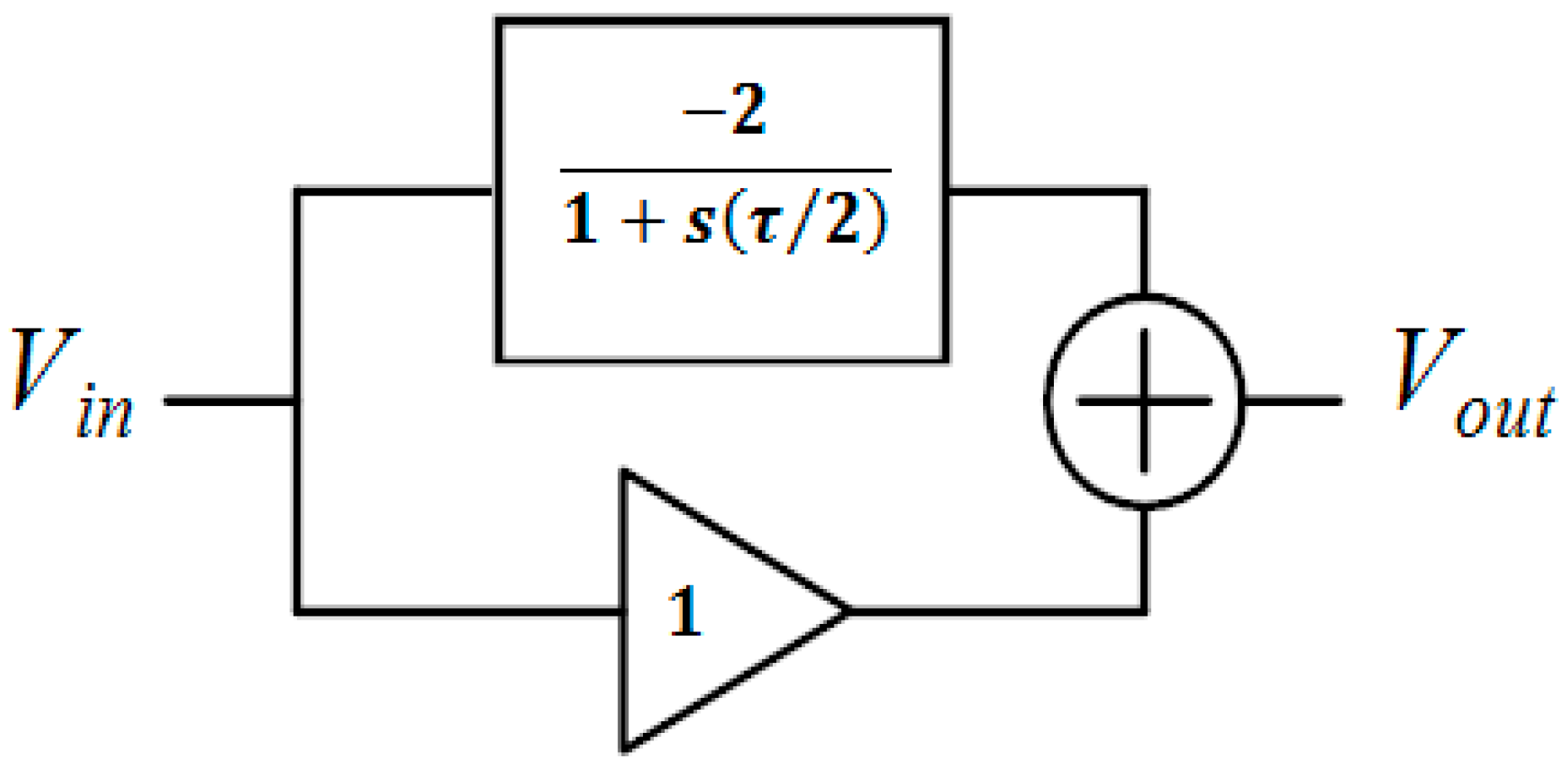
Figure 1 shows the block level of the first-order voltage-mode all-pass filter. As shown, a first-order all-pass filter can be approximated by the combination of two sections: a low-pass section with a DC gain of 2 and a unity gain section [24]. Therefore, its ideal transfer function is given as:
where is the time delay. Ideally, the gain of the transfer function is 1 and its phase is linear versus the frequency.
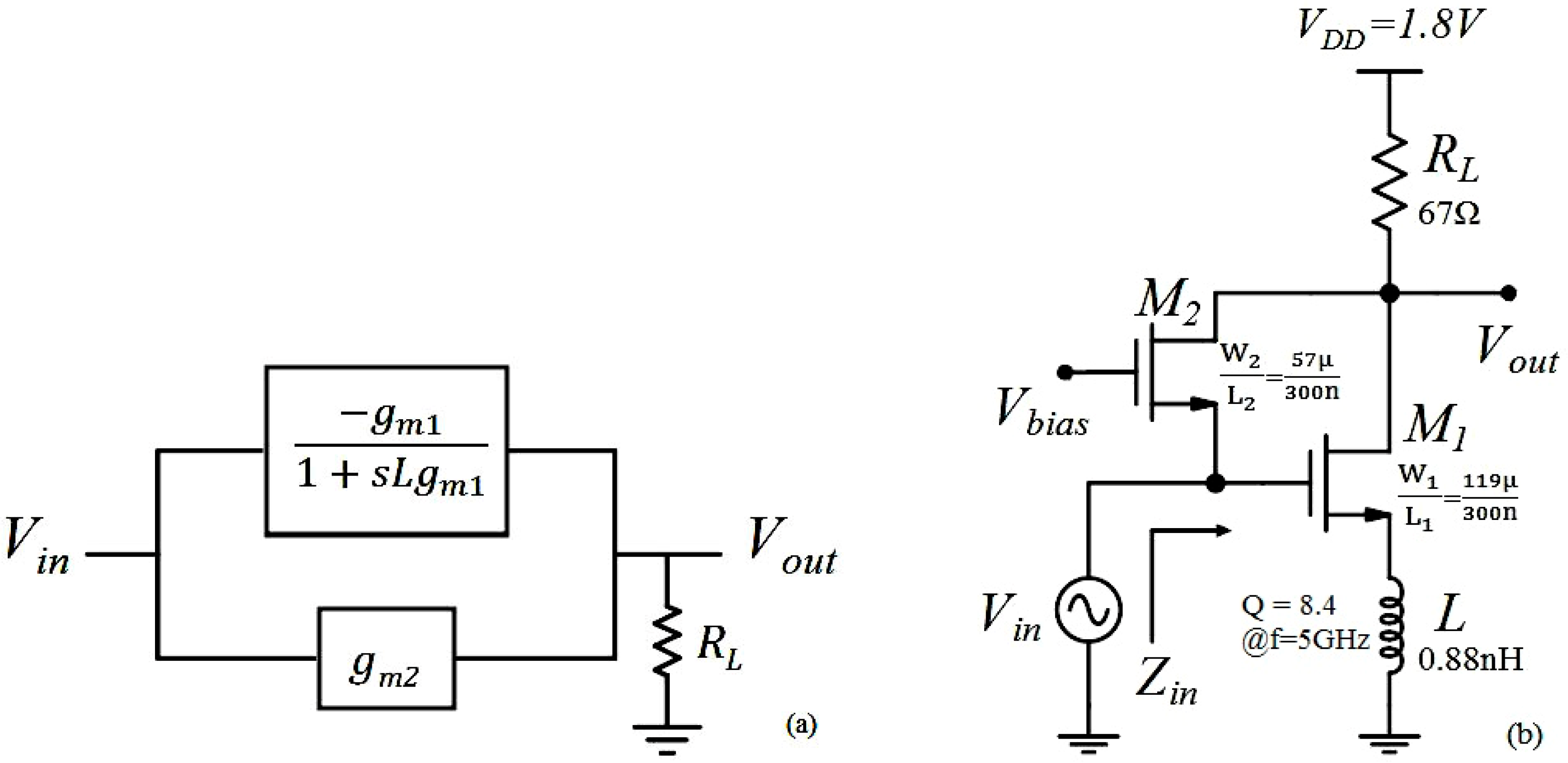
Figure 2 illustrates the block diagram and schematic of the proposed broadband first-order voltage-mode all-pass filter. In this filter, transistor , inductor , and resistor form the low-pass part, while transistor and resistor comprise the unity-gain part. In other words, and are, respectively, common-source (CS) and common-gate (CG) configurations to convert the input voltage signal into current. At the output node, the drain currents of and are subtracted to realize an all-pass function. Then, the output signal will be converted back to voltage by the load resistor .
Ignoring the parasitics of the transistors (the parasitic effects will be assessed in Section 3) for simplicity, the transfer function of the proposed first-order all-pass filter can be determined by:
where and are the transconductances of and , respectively. If and , an all-pass structure will be realized with the same frequency of the left-plane pole and right-plane zero, resulting in twice the phase and group delay responses of an all-pass circuit. As a consequence, the transfer function in (2) can be simplified as:
The pole/zero frequency and phase response of the first-order all-pass filter can be given as:
respectively, and, thus, group delay response is expressed by:
where is the angular frequency related to the frequency through . The group delay is approximately equal to at low frequencies. However, this group delay is practically affected by parasitic inductances stemmed from, e.g., bonding wire and PCB and, thus, its value will be increased. The input impedance of the proposed all-pass filter can be simply approximated by considering the Miller effect on the parasitic capacitances of the transistor plus given as:
which its value affects the next delay stage for cascading purposes.
3. Circuit Optimization and Tunability
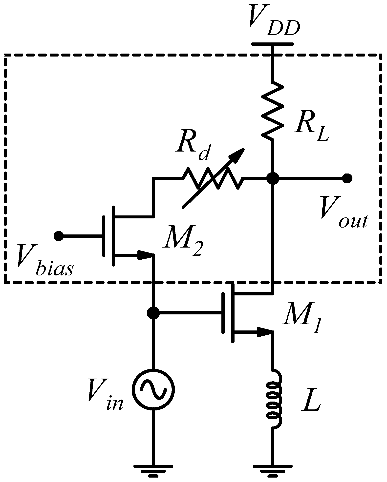
In order to contribute to the linearity and increase the operating frequency of the proposed all-pass filter, a variable resistor is added to the unity-gain path as shown in Figure 3. In this case, a discrete tuning of delay can be carried out by changing the value of and the bias voltage of as well, which adjusts . The can be implemented by a switched resistors bank which can be implemented by CMOS transistors, with great ease.
The transfer function of the CG transistor of (the part inside the dotted box) is, therefore, given as:
Its value for low and high frequencies is and , respectively. Hence, the will affect the frequency response of the proposed filter at higher frequencies. Note that (i.e., the unity gain section) is no longer equal to 1 at high frequencies, but via varying the bias voltage of , changes and, therefore, the two conditions and will be satisfied.
Non-Ideality Analysis
To analyze accurately the performance of the proposed all-pass filter in Figure 3 at high frequencies, the finite output impedances () and parasitic capacitances ( and ) of the transistors and should be considered. Therefore, the transfer function in (2) can be rewritten as:
If , , and , the transfer function in Equation (9) can be simplified as:
which includes additional parasitic poles and zero. These parasitic high-frequency poles stemmed from and , which are located at and respectively, are far beyond the dominant pole in Equation (4) since the values of and are small. Moreover, the additional right-plane zero is located at considerably higher frequencies, as well.
Additionally, small-signal analysis conducted on the proposed all-pass circuit indicates that the third parasitic pole stemmed from will be located at:
which is far beyond the dominant pole in Equation (4). It can be noted that the order of the proposed circuit will increase and convert to the second one if the absolute value of , which is process-dependent, is large enough. Consequently, choosing an appropriate CMOS process can reduce the effect of the on the frequency response of the circuit.
4. Results
The proposed first-order all-pass filter is designed in a standard 180-nm TSMC CMOS process and results are obtained using Virtuoso Cadence. The proposed all-pass filter is simulated without and with the . The power consumption of the proposed broadband true-time-delay cell is only 10 mW from a 1.8-V supply voltage.
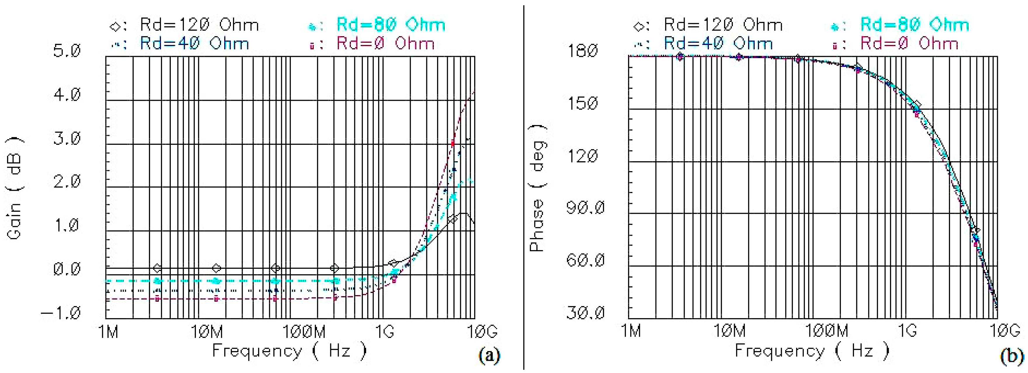
Figure 4 shows the gain and phase responses of the proposed filter under different values of the . As it can be observed, the gain of the proposed filter without the (i.e., ) is almost −0.5 dB due to the existence of the parasitic capacitors and finite output impedances of the transistors. Furthermore, the proposed filter does not achieve desired (flat) gain responses at higher frequencies, whereas by varying the value of the , better gain responses are proved at these frequencies. As seen, the pole/zero frequency of the proposed circuit with is 5 GHz (i.e., the point where phase is ), indicating a 14% bandwidth improvement compared to once (i.e., 4.4 GHz).
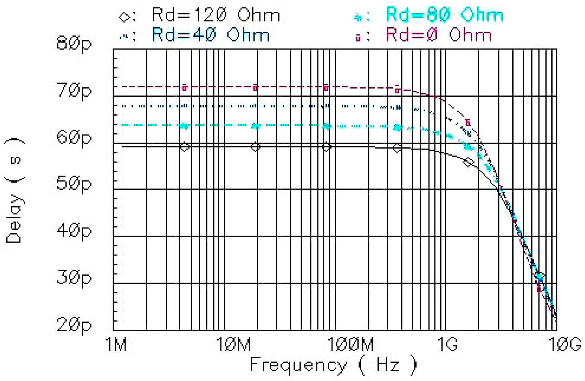
The group delay responses of the proposed all-pass filter for different values of the are shown in Figure 5. As it can be seen, the delay can be controlled by varying the . The group delay is equal to about 59 ps, when . This group delay value is very close to the theoretical one in Equation (6), with an error of around 11%.
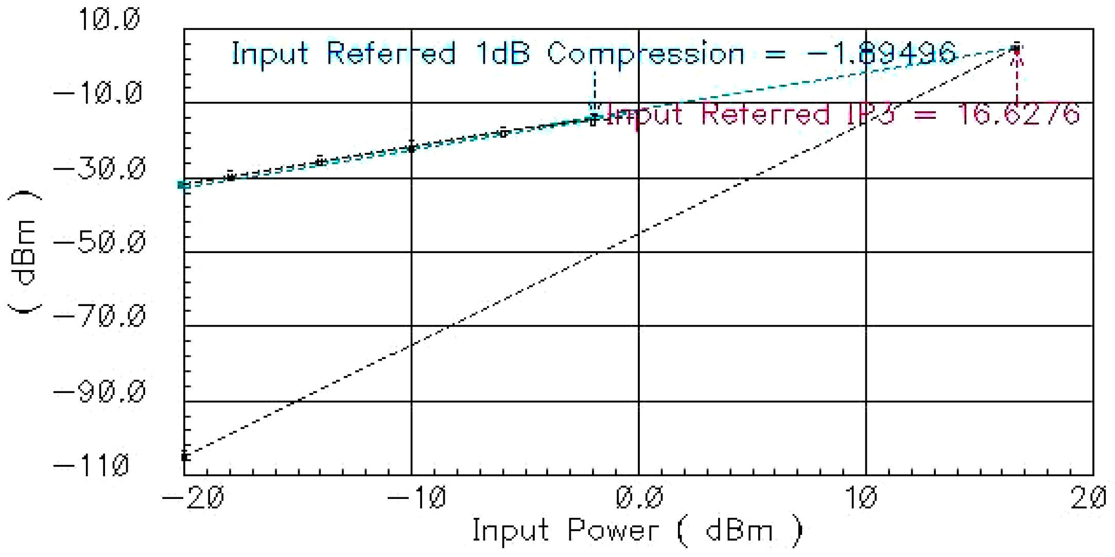
In Figure 6, the input-referred noise response of the all-pass filter is shown when . The input-referred noise value is approximately 2.36 nV/sqrt (Hz) by the frequency of 1 GHz. Figure 7 shows the noise figure of the proposed all-pass filter with , which is <15 dB over the frequency band. The input-referred 1-dB compression point and input-referred third-order intercept point (IIP3) responses of the first-order all-pass filter with are shown in Figure 8. The input-referred and IIP3 are −1.9 dBm and 16.6 dBm at 2.5 GHz, respectively.
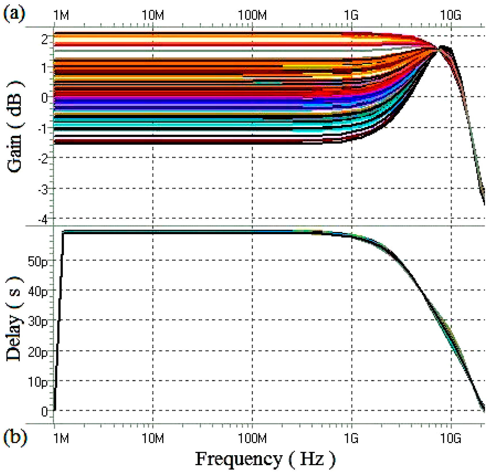
Since the amount of group delay is affected by the mismatch and is basically process, voltage, and temperature (PVT) dependent, we should therefore consider the effect of these variations on the proposed true-time-delay cell. Figure 9 illustrates Monte Carlo simulation results, which are performed with a Gaussian distribution and 100 iterations, when . As it can be seen, the difference between group delay responses due to the mismatch is very small. Although the gain, , and IIP3 will be affected by the mismatch, these variations can be minimized by changing the bias voltage of . The group delay responses of the proposed filter with for different supply voltages and temperatures are shown in Figure 10. The delay degrades by 15% because of the temperature variations.
A comparison between recently reported voltage/current all-pass filters and the proposed true-time-delay cell is presented in Table 1. Comparing the results of the first-order voltage-mode all-pass filters, the proposed filter has improved the frequency range compared to the filter in [15]. Moreover, the power consumption and delay tuning can be highlighted and compared with the filter in [22], in which the delay could not be tuned.
5. Discussion
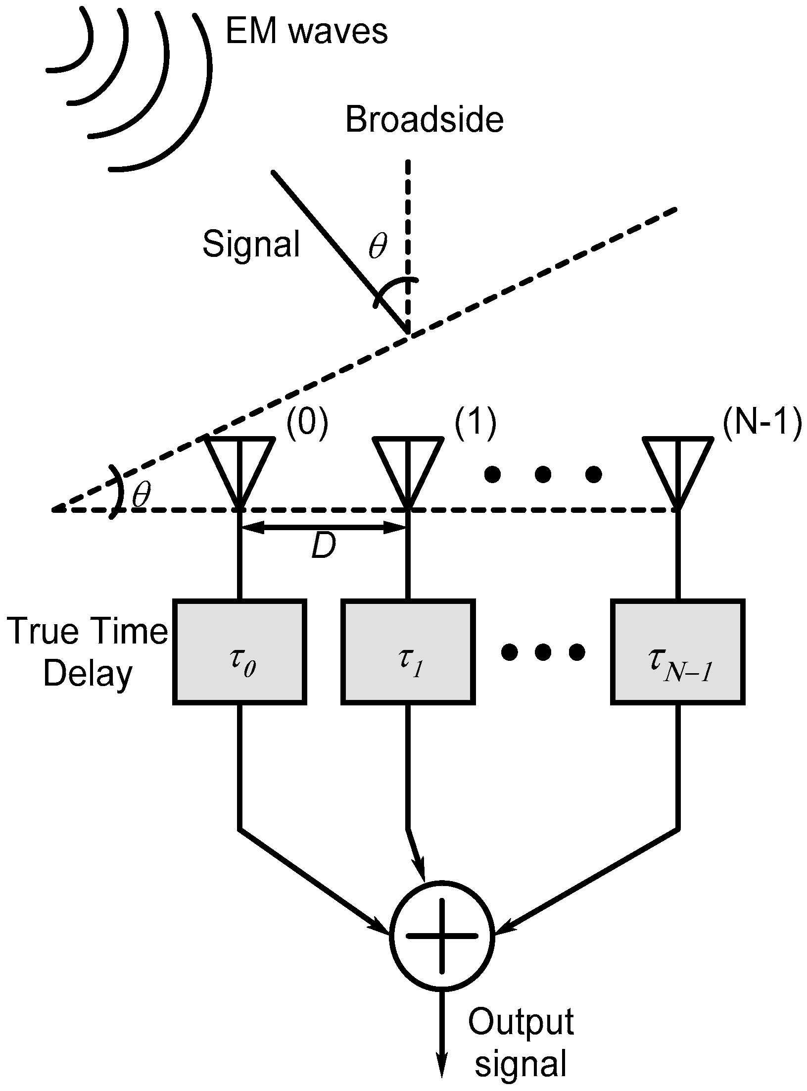
Compared to the bulky LC delay lines, active filters can be good alternatives to approximate delays as these filters occupy smaller area. This paper presents a broadband first-order voltage-mode all-pass filter as an active circuit. Via an optimization technique, 14% bandwidth extension is achieved. The proposed first-order all-pass filter demonstrates a flat group delay of approximately 60ps through a bandwidth of 5 GHz, while consuming merely 10 mW power. Unlike the active all-pass filter in [22], the proposed filter has a DC-gain of 1 in its voltage transfer function and consequently there is no need for the gain adjustment via additional circuits or components. Furthermore, the proposed circuit proves a frequency range wider than that of the reported active filter in [15] (pre-layout pole frequency of 2.63 GHz), however at a larger area. The proposed all-pass filter is almost linear and achieves the input-referred of −1.9 dBm and the input-referred IIP3 of 16.6 dBm. We will employ the proposed all-pass filter-based true-time-delay cell in analog RF beam-forming antennas for communication applications in our future work (see Figure 11). In timed-array receivers, tunable true-time-delay cells are exploited to align broadband signals received from a particular direction (θ).
Author Contributions
S.R.A. designed the circuit, and performed the theoretical analyses and simulation; and all authors wrote the paper.
Funding
This research received no external funding.
Conflicts of Interest
The authors declare no conflict of interest.
References
- Buckwalter, J.; Hajimiri, A. An active analog delay and the delay reference loop. In Proceedings of the IEEE Radio Frequency Integrated Circuits (RFIC) Systems, Fort Worth, TX, USA, 6–8 June 2004. [Google Scholar]
- Wang, Z. A Fully integrated W-band beamformer in 0.13 μm SiGe BiCMOS technology based on distributed true-time-delay architecture. In Proceedings of the IEEE International Nanoelectronics Conference (INEC), Chengdu, China, 9–11 May 2016. [Google Scholar]
- Perera, S.M.; Ariyarathna, V.; Udayanga, N.; Madanayake, A.; Wu, G.; Belostotski, L.; Wang, Y.; Mandal, S.; Cintra, R.J.; Rappaport, T.S. Wideband N-beam arrays using low-complexity algorithms and mixed-signal integrated circuits. IEEE J. Sel. Top. Signal Process. 2018, 12, 368–382. [Google Scholar] [CrossRef]
- Mailloux, R.J. Phased Array Antenna Handbook, 2nd ed.; Artech House: Norwood, MA, USA, 2005; ISBN 1-58053-689-1. [Google Scholar]
- Van Trees, H.L. Optimum Array Processing: Detection, Estimation, and Modulation Theory; Wiley: New York, NY, USA, 2002; ISBN 0-471-09390-4. [Google Scholar]
- Madanayake, A.; Ariyarathna, V.; Udayanga, N.; Belostotski, L.; Perera, S.K.; Cintra, R.J. Design of a low-complexity wideband analog true-time-delay 5 Beam array in 65 nm CMOS. In Proceedings of the IEEE International Midwest Symposium on Circuits and Systems (MWSCAS), Boston, MA, USA, 6–9 August 2017. [Google Scholar]
- Schwartz, J.; Arnedo, I.; Laso, M.A.G.; Lopetegi, T.; Azana, J.; Plant, D. An electronic uwb continuously tunable time-delay system with nanosecond delays. IEEE Microw. Wirel. Compon. Lett. 2008, 18, 103–105. [Google Scholar] [CrossRef]
- Chu, T.; Roderick, J.; Hashemi, H. An integrated ultra-wideband timed array receiver in 0.13 μm cmos using a path-sharing true time delay architecture. IEEE J. Solid-State Circuits 2007, 42, 2834–2850. [Google Scholar] [CrossRef]
- Soer, M.; Klumperink, E.; Nauta, B.; van Vliet, F. A 1.5-to-5.0 GHz input-matched +2 dBm P1dB all-passive switched-capacitor beamforming receiver front-end in 65 nm CMOS. In Proceedings of the IEEE International Solid-State Circuits Conference (ISSCC), San Francisco, CA, USA, 19–23 February 2012. [Google Scholar]
- Ghaffari, A.; Klumperink, E.; Soer, M.; Nauta, B. Tunable high-q n-path band-path filters: Modeling and verification. IEEE J. Solid-State Circuits 2011, 46, 998–1010. [Google Scholar] [CrossRef]
- Lien, Y.; Klumperink, E.; Tenbroek, B.; Strange, J.; Nauta, B. A high-linearity CMOS receiver achieving +44 dBm IIP3 and +13 dBm B1dB for SAW-Less LTE radio. In Proceedings of the IEEE International Solid-State Circuits Conference (ISSCC), San Francisco, CA, USA, 5–9 February 2017. [Google Scholar]
- Li, W.; Wang, W.; Chen, Y. A 0.5–3 GHz true-time-delay phase shifter for multi-antenna systems. In Proceedings of the IEEE 2nd Advanced Information Technology, Electronic and Automation Control Conference (IAEAC), Chongqing, China, 25–26 March 2017. [Google Scholar]
- Elkind, J.; Goldberger, E.; Socher, E. 57–67 GHz highly compact bidirectional 3-bit phase shifter in 28 nm cmos. IEEE Microw. Wirel. Compon. Lett. 2018, 28, 1017–1019. [Google Scholar] [CrossRef]
- Zhang, Y.; Huang, F.; Li, T.; Tang, X.; Jiang, N. A 1 V 2.4–6 GHz 6 bit vector-sum phase shifter with very low rms phase error and gain error. Microw. Opt. Technol. Lett. 2018, 60, 2467–2471. [Google Scholar] [CrossRef]
- Garakoui, S.K.; Klumperink, E.; Nauta, B.; van Vliet, F. Compact cascadable gm-c all-pass true time delay cell with reduced delay variation over frequency. IEEE J. Solid-State Circuits 2015, 50, 693–703. [Google Scholar] [CrossRef]
- Mondal, I.; Krishnapura, N. A 2 GHz bandwidth, 0.25–1.7 ns true-time-delay element using a variable-order all-pass filter architecture in 0.13 μm cmos. IEEE J. Solid-State Circuits 2017, 52, 2180–2193. [Google Scholar] [CrossRef]
- Wijenayake, C.; Madanayake, A.; Belostotski, L.; Xu, Y.; Bruton, L. All-pass filter-based 2-D IIR filter-enhanced beamformers for AESA receivers. IEEE Trans. Circuits Syst. I Regul. Pap. 2014, 61, 1331–1342. [Google Scholar] [CrossRef]
- Chen, Y.; Li, W. Campact and broadband variable true-time delay line with DLL-based delay-time control. Circuits Syst. Signal Process. 2018, 37, 1007–1027. [Google Scholar] [CrossRef]
- Ulusoy, A.; Schleicher, B.; Schumacher, H. A tunable differential all-pass filter for uwb true time delay and phase shift applications. IEEE Microw. Wirel. Compon. Lett. 2011, 21, 462–464. [Google Scholar] [CrossRef]
- Ahmadi, P.; Maundy, B.; Elwakil, A.S.; Belostotski, L.; Madanayake, A. A new 2nd-order all-pass filter in 130 nm cmos. IEEE Trans. Circuits Syst. II Express Br. 2016, 63, 249–253. [Google Scholar] [CrossRef]
- Wijenayake, C.; Xu, Y.; Madanayake, A.; Belostotski, L.; Bruton, L. RF analog beamforming fan filters using cmos all-pass time delay approximations. IEEE Trans. Circuits Syst. I Regul. Pap. 2012, 59, 1061–1073. [Google Scholar] [CrossRef]
- Ahmadi, P.; Taghavi, M.H.; Belostotski, L.; Madanayake, A. 6-GHz all-pass-filter-based delay-and-sum beamformer in 130 nm CMOS. In Proceedings of the IEEE International Midwest Symposium on Circuits and Systems (MWSCAS), College Station, TX, USA, 3–6 August 2014. [Google Scholar]
- Maheshwari, S. Tuning approach for first-order filters and new current-mode circuit example. IET Circuits Devices Syst. 2018, 12, 478–485. [Google Scholar] [CrossRef]
- Bult, K.; Wallinga, H. A cmos analog continuous-time delay line with adaptive delay-time control. IEEE J. Solid-State Circuits 1988, 23, 759–766. [Google Scholar] [CrossRef]
- Ahmadi, P.; Belostotski, L.; Madanayake, A.; Haslett, J.W. 0.96-to-5.1 GHz 4-element spatially analog IIR-enhanced delay-and-sum beamformer. In Proceedings of the IEEE International Microwave Symposium (IMS), Honolulu, HI, USA, 4–9 June 2017. [Google Scholar]
- Chen, Y.; Li, W. An ultra-wideband pico-second true-time-delay circuit with differential tunable active inductor. Analog Integr. Circuits Signal Process. 2017, 91, 9–19. [Google Scholar] [CrossRef]
Figure 1.
Block diagram of the first-order all-pass filter.

Figure 2.
(a) Block diagram and (b) schematic of the proposed first-order all-pass filter.

Figure 3.
The optimization and tunability technique.

Figure 4.
Simulated results for (a) gain response and (b) phase response of the proposed first-order all-pass filter under different values of the .
Figure 4.
Simulated results for (a) gain response and (b) phase response of the proposed first-order all-pass filter under different values of the .

Figure 5.
Simulated group delay responses of the proposed first-order all-pass filter under different values of the .
Figure 5.
Simulated group delay responses of the proposed first-order all-pass filter under different values of the .

Figure 6.
Simulated input-referred noise response of the proposed first-order all-pass filter.

Figure 7.
Simulated noise figure response of the proposed first-order all-pass filter.

Figure 8.
Simulated input-referred and input-referred IIP3 responses of the proposed first-order all-pass filter.
Figure 8.
Simulated input-referred and input-referred IIP3 responses of the proposed first-order all-pass filter.

Figure 9.
Monte Carlo simulation results for (a) gain response and (b) group delay response of the proposed first-order all-pass filter.
Figure 9.
Monte Carlo simulation results for (a) gain response and (b) group delay response of the proposed first-order all-pass filter.

Figure 10.
Simulated group delay responses of the proposed first-order all-pass filter for (a) different supply voltages and (b) different temperatures.
Figure 10.
Simulated group delay responses of the proposed first-order all-pass filter for (a) different supply voltages and (b) different temperatures.

Figure 11.
Block diagram of an N-element timed-array receiver.


Table 1.
Performance summary and comparison between broadband all-pass filters.
| Reference | Technology | Mode | Order | Frequency (GHz) | Max. Delay (ps) | P1dB (dBm) | IIP3 (dBm) | Power (mW/V) |
|---|---|---|---|---|---|---|---|---|
| [15] | 140-nm CMOS | Voltage | 1st | 1–2.5 | 61 1 | N/A | N/A | 10 2/1.5 |
| [19] | SiGe2RF HBT | Voltage | 2nd | 3–10 | 75 | −1 | N/A | 38.8/2.5 |
| [20] | 130-nm CMOS | Voltage | 2nd | 6 | 55 | −5.5 | 2 | 18.5/1.5 |
| [22] | 130-nm CMOS | Voltage | 1st | 9 | 49 3 | −2 | 8.5 | 20.4/1.5 |
| [25] | 130-nm CMOS | Current | 1st | 0.3–5.1 | 82 | N/A | N/A | 6.15/1.5 |
| [26] | 180-nm CMOS | Voltage | 2nd | 3–12 | 8.5 | 14.6 | 22.6 | 12/1.8 |
| This work | 180-nm CMOS | Voltage | 1st | 5 | 59 4 | −1.9 | 16.6 | 10/1.8 |
1 A maximum delay of 550 ps was achieved by three fine and six coarse delays. 2 A maximum power of 90 mW was consumed by three fine and six coarse delays. 3 Pre-layout group delay of 33 ps expected for the filter. 4 Simulated group delay value can be increased by varying the value of variable resistor in the proposed filter.
© 2018 by the authors. Licensee MDPI, Basel, Switzerland. This article is an open access article distributed under the terms and conditions of the Creative Commons Attribution (CC BY) license (http://creativecommons.org/licenses/by/4.0/).
Share and Cite
MDPI and ACS Style
Aghazadeh, S.R.; Martinez, H.; Saberkari, A. 5GHz CMOS All-Pass Filter-Based True Time Delay Cell. Electronics 2019, 8, 16. https://doi.org/10.3390/electronics8010016
AMA Style
Aghazadeh SR, Martinez H, Saberkari A. 5GHz CMOS All-Pass Filter-Based True Time Delay Cell. Electronics. 2019; 8(1):16. https://doi.org/10.3390/electronics8010016
Chicago/Turabian StyleAghazadeh, Seyed Rasoul, Herminio Martinez, and Alireza Saberkari. 2019. "5GHz CMOS All-Pass Filter-Based True Time Delay Cell" Electronics 8, no. 1: 16. https://doi.org/10.3390/electronics8010016
Note that from the first issue of 2016, this journal uses article numbers instead of page numbers. See further details here.